

Design Perfection from Concept to Tape-out
Booth #1617 at DAC25 - June 23-25, 2025
Join us to learn how Altair’s world-class solutions are powering perfect semiconductor design.
The semiconductor industry operates at an accelerated pace, in which every second saved is a competitive advantage. You must rely on solutions that complement each other at every step in the semiconductor design process to beat others to market.
Altair’s solutions empower organizations to design perfection from concept to tapeout. From silicon debugging tools for integrated circuit (IC) designs to multiphysics analysis of 3D IC and chiplet design simulations, Altair offers the complete solutions set. With the fastest high-throughput workload manager available and an advanced workflow analysis tool, designers can trust Altair with every challenge.
Speak with an expert at DAC.
Book meetingLive Presentations
Transform the semiconductor industry.
Design perfection from the start with advanced silicon debugging, rapid 3D IC electrothermal-mechanical simulations, and the industry’s only on-demand digital simulator for semiconductor electronic functional verification. Avoid costly dependencies and optimize infrastructure utilization with HPC workload and workflow optimization and bring reliable designs to market faster.
Join us for live presentations throughout the conference featuring industry leaders and technology experts.
11:30 am - 12:00 pm | Altair SimLab: Integrated Environment for Multiphysics Modeling and AI-Driven Reliability Prediction in 3D IC Systems
Iyad Rayane, Senior Technical Specialist ESD, Altair
This solution provides a comprehensive environment for modeling and pre/post-processing of 3D Integrated Circuit (3D IC) structures, enabling robust multiphysics analysis including thermal, mechanical, and electrical domains. It interfaces with advanced AI-driven physics capabilities to predict system lifespan rapidly and accurately, significantly reducing simulation runtime. Additionally, the environment supports thermal-aware chiplet floorplanning, optimizing thermal dissipation at the system level to enhance reliability and performance. This integrated approach facilitates early design exploration and informed decision-making for next-generation heterogeneous 3D ICs.
01:00 pm - 01:30 pm | Altair NavOps: Bursting Workload demand to the cloud!
Yohan Bouvron, Support Engineer, Enterprise Computing, Altair
Engineers want as little wait time as possible to run their workloads and management wants the highest possible utilization of the systems. Altair’s NavOps + Accelerator can provide an optimal solution for both.
02:00 pm - 02:30 pm | FlowTracer Refresh – A new era of vendor-agnostic design automation platform
Dee Lin, Lead Principal Solution Architect, Altiar
Since its inception, FlowTracer has become a popular commercial ASIC/SoC design automation platform among the top semiconductor companies. This year, Altair is launching 2025 release with major GUI and feature-rich modernization. We will go through these major features and improvements in this presentation.
11:30 am - 12:00 pm | Altair's InsightPro for HPC and License Analytics: A complete solution to HPC resource and licensing analytics
Yohan Bouvron, Support Engineer, Enterprise Computing, Altair
Efficient use of HPC resources and vendor license is top of mind for many Engineering/Design team management. Altair’s InsightPro can help with that.
01:00 pm - 01:30 pm | Scalable ECAD Modeling for 3D IC Packaging and Silicon Interposers
Iyad Rayane, Senior Technical Specialist ESD, Altair
The emergence of three-dimensional integrated circuits (3D ICs) has revolutionized semiconductor technology by enabling higher performance, reduced power consumption, and increased integration density.
However, this advancement introduces significant challenges for IC packaging and silicon interposers.
The complexity of 3D IC structures, including through-silicon vias (TSVs), micro-bumps, and redistribution layers (RDLs), imposes stringent requirements on electrical, thermal, and mechanical performance. These factors make accurate modeling and analysis increasingly difficult in multiphysics simulation tools.
Additionally, as IC package and silicon interposer designs grow more intricate, the sheer size and detail of ECAD models present a major bottleneck for existing simulation tools.
Current modeling approaches often fail to efficiently handle the large-scale geometries and fine-grained features of modern IC packaging, requiring a paradigm shift in how multiphysics tools import, process, and analyze these models.
This presentation explores the challenges associated with 3D IC packaging and interposer design and explicitly highlights the need for new modeling approaches to accommodate large ECAD models.
02:00 pm - 02:30 pm | Visualize and Simplify: Breaking Down SPICE Netlists
Pascal Bolzhauser, Senior Manager Software Development, Altair
A primary Silicon Debug Tools’ advantage is converting a SPICE netlist into easy-to read-circuit diagrams. Designers are empowered to see the schematics of their circuits in clear detail, generate debugging views on the fly, making it easier to identify critical paths and optimize their SoC design or IP components.
Altair’s silicon debugging tools solution offers a high-performance and memory-efficient database that easily handles designs for large integrated systems.
With tool configuration and workflow automation, engineers can define custom checks, ensuring that optimized, validated, and reliable designs reach the manufacturing stage faster.
Latest Resources

A Technology Leap for Higher Throughput and Utilization
Presentation by Peter Dobszai, VP High Tech Vertical EMEA at Altair as part of Altair's Future.Industry 2025 conference.
Watch Now
Six Smarter Scheduling Techniques for Optimizing EDA Productivity
Verification engineers and IT managers are constantly looking for new sources of competitive advantage. In this paper, we discuss six valuable techniques to help improve design center productivity.
Read now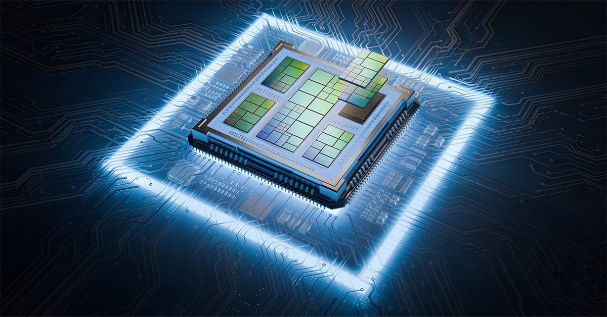
Altair SimLab: 3D Digital Twin for 3D IC and Advanced IC Packaging
Altair SimLab, featuring multiphysics and automation capabilities, is designed for 3D integrated circuit (IC) and advanced IC packaging, creating a 3D digital twin of the entire 3D IC system.
Check it outMeet Altair® HPCWorks®: Optimized EDA Job Scheduling for Semiconductor Design
Accelerate the design exploration and verification process with Altair enterprise computing solutions for semiconductor design. Engineering teams rely on Altair to beat competitors to market with the most comprehensive and performant solution set on the market.
You need your environment to maximize resources and run faster than the competition. Trust the industry’s leading job scheduler to meet the complex demands of semiconductor design with scalability, adaptability, and efficiency.
Chip design is increasing in complexity every day and requires visualization tools to match. Flow visualization tools that provide analysis and troubleshooting capabilities will optimize compute resources for a faster, more effective design process at every step.
Licenses are a costly investment and often in high demand among chip designers on any given team. Managing these tools effectively can speed up time-to-market while achieving a better ROI. Monitor their usage and maximize license allocation through sharing for increased efficiency and real-time insight.
I/O profiling helps organizations determine the optimal compute environment for different types of ESD applications and resources. Monitoring applications increases visibility and enables informed planning, and application profiling can help solve deployment issues quickly.
Hardware emulators are an expensive component of the chip design process. Address all aspects of emulation flow including design compilation, emulator selection, and software and regression tests with a job scheduler designed for hardware emulators.


Complete Electronic System Design Solution
Altair offers best-in-class multi-disciplinary simulation, AI, HPC scheduling and workflow dependency management. Streamline the semiconductor design process with silicon debugging tools and cutting-edge 3-D IC multiphysics solutions. In addition, chip to board to system ESD solutions streamline your processes to eliminate design iterations, ensure reliability, and reduce time-to-market.
Offsetting the higher design and manufacturing costs associated with increasing chip complexity and 3D IC chip design is possible with efficient design and debugging tools that can streamline and minimize design repetitions.
Dependable, tested solutions should offer quick visualization capabilities for spotting cause-and-effect patterns and provide rapid debugging solutions for varied system-on-chip designs. These diverse designs can include analog components, third-party Intellectual Property (IP), multi-core processors, and chiplet-based designs that all require a versatile analysis and debugging solution for rapid design evaluation.
Debug tools support engineers and optimize designs, moving devices into production earlier and with a higher degree of confidence.
Developing electronic products that withstand the structural, operational, and environmental requirements of everyday use or misuse requires a team effort. Altair's cutting-edge 3-D IC multiphysics solutions and intuitive ESD multiphysics workflows that consider electrothermal, cooling, vibration, noise, solder fatigue, and structural effects ensure chip, PCB, and system-level reliability. With process-oriented ESD simulation workflows in a collaborative development environment, designers and engineers can shorten development cycles and costs to deliver innovative and reliable products faster.
Some form of power converter is present in nearly all modern electronics, from small cell phone chargers to multi-megawatt propulsion systems. As performance requirements become more demanding, circuit simulation plays a strategic role in the schematic capture phase of EDA workflows for competitive designs. Companies that an adopt industry-proven solution like PSIM to simulate power electronic systems can readily optimize energy efficiency and thermal management performance while evaluating component interaction and overall system responses based on operating conditions and environmental factors. And with efficient power electronic simulation workflows, companies can explore new architecture, materials, and control strategies for complex systems faster, helping to drive their next innovations.
Rapid modeling and visualization for electrical circuit systems is essential to gain rapid insights into circuit design and avoid costly design errors. Altair HyperSpice, with access to Spice libraries for fast AC, DC, and Transient simulations, is fully integrated into a flexible system-wide simulation solution, helping companies innovate faster.